
SEMICONDUCTOR PACKAGING
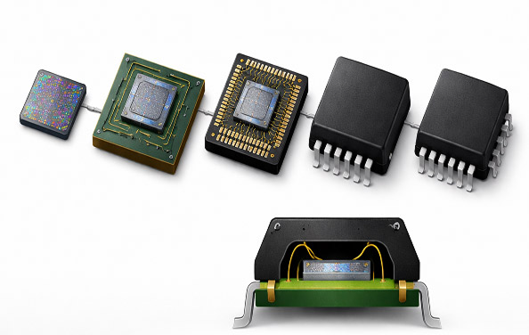
OVERVIEW
Pioneering Advanced Semiconductor Packaging in India
Powering the technologies of tomorrow, our semiconductor capabilities span advanced System-in-Package (SiP) design and manufacturing, cutting-edge silicon photonics, and tailored industry solutions.
From high-performance ASIC design to efficient power integration and precision radio frequency and microwave assemblies, we bring together innovation, scalability, and reliability to solve complex engineering challenges and accelerate next-generation product development across industries.
A division of the BSE & NSE listed izmo limited, izmomicro is shaping the future
of semiconductor packaging in India with precision engineering, silicon photonics innovation,
and world-class manufacturing infrastructure.
Deep Tech Innovation
Silicon photonics and co-packaged optics
India-First Manufacturing
Bengaluru HQ with Class 1000 cleanroom
IP-Secured by Design
SiP architecture with built-in IP protection
Global Footprint
India, US, UK, Germany, Belgium, France




Advancing Next-Generation Photonic Processors
izmomicro - a subsidiary of izmo Ltd., specializing in semiconductors, is the exclusive industry partner in the IIT Madras Photonic Chip Packaging Initiative. The partnership focuses on developing next-generation programmable photonic processors (FPPGA), advancing photonic integration for quantum and AI-driven applications, and driving innovative silicon photonics solutions for high-speed telecom and computing technologies.
CORE CAPABILITIES
From Concept to Commercialization
Our services span the entire product lifecycle - enabling rapid innovation and reliable deployment.
01 — DESIGN
Design & Simulation
Use advanced simulation tools and deep domain expertise to design high-performance photonic solutions and SiPs optimized for performance and reliability from the outset.
02 — VALIDATION
Testing & Packaging
Deliver advanced photonic packaging and SiPs supported by rigorous testing to ensure compliance and meet specific application requirements.
03 — PRODUCTION
Manufacturing
Enable flexible, scalable manufacturing - from low-volume research builds to full-scale commercial production.
CAPABILITIES
Semiconductor Solutions Across Sectors
IC Packaging & SiP
Advanced System-in-Package and Multi-Chip Module assembly for high-density, high-performance industrial and aerospace applications.
Silicon Photonics
Complete photonic lifecycle - design, simulation, testing, packaging, and manufacturing for advanced optical interconnects.
RF & MW Assemblies
High-intensity Radio Frequency and Microwave assemblies for defense, telecom, and industrial applications.
ASIC
Tailored solutions enabling fabless ASIC design firms to achieve optimized performance, power efficiency, and form factor.
Power Integration
Advanced power module packaging for automotive, industrial, renewable energy, and high-reliability markets.
Co-packaged Optics
Cutting-edge optical solutions integrating photonic and electronic chips for ultra-high-bandwidth data center and AI infrastructure.
INDUSTRIES WE SERVE
Advanced Manufacturing Expertise
Manufacturing excellence with SiP and SMT solutions, delivered from our state-of-the-art cleanroom in Whitefield, Bangalore.
High-Precision Capabilities
High-precision packaging powered by advanced assembly, bonding, molding, and hybrid substrate technologies.
Industry-Grade Quality
SiP and MCM assemblies designed to meet stringent requirements of high-tech industrial and aerospace applications.
BREAKTHROUGH
High-Power Motor Control
Technology
IN-HOUSE R&D
With Prestigious DSIR
Recognition
84%
Footprint Reduction in Space-Grade
Packaging
PARTNERSHIP
izmo Ltd × IIT Madras for Photonic
Chip Packaging
SIP DESIGN & MANUFACTURING
Advanced Packaging for Mission-Critical Applications
At izmo, we deliver advanced System-in-Package (SiP) solutions with end-to-end semiconductor packaging and manufacturing capabilities. From substrate design to full-scale production, we support every stage of the product lifecycle - engineering samples, prototyping, pilot runs, qualification, and high-volume manufacturing.
WHY PARTNER WITH US
Multidisciplinary Expertise Backed by Infrastructure
Partnering with izmo gives you access to multidisciplinary expertise backed by specialized skills and advanced tools that address thermal management, electrical interference, and rigorous testing to minimize design risks.
ENGINEERING APPROACH
A Three-Pronged Approach to Industry-Ready Solutions
- Flip chip
- 3D packaging
- MEMS packaging
- Thin die and brittle die
- Hermetic sealing
- Optical assembly
- Package design - organic, LTCC, HTCC, thermally enhanced
- SI & PI analysis
- Thermal and thermo-mechanical analysis
- EMI/EMC analysis
- Packaging: QFN, BGA, PQFP, CQFP, DIP, Metal Can, COB
- MCM
- System-in-Package
- Thick film hybrid microcircuits
- Thin film hybrid circuits
- RF and microwave modules
SILICON PHOTONICS
The Rising Wave of Silicon Photonics
Silicon photonics is revolutionizing high-speed data transmission, AI computing, and next-gen communication networks. At izmo, we provide world-class silicon photonics packaging, assembly, and manufacturing solutions, addressing the critical challenges of optical alignment, thermal management, and heterogeneous integration.
KEY BUSINESS SEGMENTS FOR SILICON PHOTONICS
Hyperscale data centers & cloud
computing
Quantum computing & secure
communications
AI & optical computing
Next-gen telecommunications
Biomedical imaging & optical
sensing
CAPABILITIES & MANUFACTURING EXPERTISE
izmo's Silicon Photonics Packaging Ecosystem
With over a decade of experience in IC packaging and System-in-Package (SiP), izmo has developed a state-of-the-art silicon photonics packaging and manufacturing ecosystem. As India's first and only silicon photonics packaging provider, we combine advanced facilities with strong industry collaborations.
Precision Silicon Photonics Assembly & Packaging
Advanced heterogeneous SiP solutions for photonic integration. Sub-micron active alignment of fiber arrays, waveguides, and laser sources. High-speed electrical and optical interconnects with low-loss coupling techniques for efficient fiber attachment and photonic waveguide integration.
High-Performance Package Design
Effective thermal management through heat spreaders, thermoelectric cooling (TEC), and optimized material selection. Enhanced signal and power integrity for high-speed applications. 2.5D and 3D packaging with optical and RF co-packaging for high-bandwidth, low-latency performance.
Mid-Volume Silicon Photonics Manufacturing
Scalable manufacturing with fully optimized mid-volume production lines tailored for photonic devices. Custom test and validation solutions for high-yield, reliable packaging. Deep expertise in co-packaged optics for AI, cloud, and data center applications.
Exclusive Industry Collaboration with IIT Madras
izmomicro is the exclusive industry partner in the IIT Madras Photonic Chip Packaging Initiative, collaborating on next-generation programmable photonic processors (FPPGA) and advancing photonic integration for quantum and AI-driven applications.

INDUSTRY SOLUTIONS
Tailored Solutions for Every Application
From advanced IC packaging for fabless ASIC firms to high-performance power modules and precision RF assemblies — customized to align with your budget, performance goals, and size requirements.
PACKAGE PORTFOLIO
ASIC SOLUTIONS
Advanced IC Packaging for Fabless Design Firms
Our advanced IC packaging services empower fabless ASIC design firms to achieve optimal performance, power efficiency, and compact form factors. Each solution is thoughtfully customized to align with a client's specific budget, performance goals, and size requirements.

POWER INTEGRATION
High-Performance Packaging for Energy-Intensive Applications
At izmo, we deliver advanced power module packaging solutions for automotive, industrial, renewable, and high-reliability markets. Our expertise in motor control, power conversion, and energy management ensures optimized electrical performance, thermal efficiency, and scalable manufacturing.
Specialists in power electronics
packaging
Proven track record in technology
integration
Comprehensive development
support
Trusted across various sectors
Certified world-class infrastructure
BLDC Motor Driver Modules
Compact, rugged packages designed for low conduction losses and reliable high-current handling.
Hex Bridge Modules
Configurable half-bridge and full-bridge topologies suitable for robotics and power tools.
IGBT Power Modules
High-voltage modules with enhanced reliability for demanding operating conditions.
- Direct-Bonded Copper (DBC)
- Direct-Bonded Aluminum (DBA)
- Active Metal Brazing (AMB)
- Insulated Metal Substrate (IMS)
- Void-free soldering with optimized fluxes
- Double-sided cooling architecture
- High-conductivity materials & thermal interface management
- Lid/spreader designs for long-term operation
RF & MW ASSEMBLIES
Precision Packaging for High-Frequency Performance
Our expertise in Radio Frequency (RF) and Microwave (MW) assemblies spans a wide range of package families - from open-cavity QFN for sensitive analog and mixed-signal devices to flip-chip BGAs and complete RF modules, all customized for specific applications.
Expertise
Capabilities
Support
Experience
Infrastructure
IC Architecture for Quick-To-Market Applications
Open-Cavity QFN Packages
Ideal for RF front-end devices like MMICs, power amplifiers, and LNAs. Enables precision wire bonding with minimal parasitics, superior RF and thermal performance, multiple bonding materials, and high-reliability assembly.
Molded QFN Packages
Fully encapsulated QFN with 50Ω impedance-optimized design for reliable RF performance up to mmWave bands. Supports high-volume, cost-efficient manufacturing with flexible configurations for power and RF co-integration
Flip-Chip BGA (FCBGA)
High-frequency routing with short interconnects for low-loss high-bandwidth using organic/ABF substrates. Enables advanced MMIC and RF SoC integration with multi-die, high-I/O, and antenna-in-package (AiP) configurations.
RF Module Assembly
Compact multi-chip RF systems integrating filters, amplifiers, antennas, and passives using advanced SiP techniques. Supports diverse applications from 5G and IoT to radar and defense with flexible reliability options.
READY TO BUILD WHAT'S NEXT?
Partner with India's
Semiconductor Pioneer
Whether you need advanced SiP packaging, silicon photonics integration, or precision RF assemblies - izmo Ltd has the technology, infrastructure, and expertise to deliver.